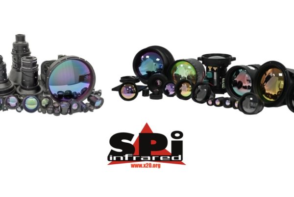
Exocet SWIR short wave infrared InGaAs camera
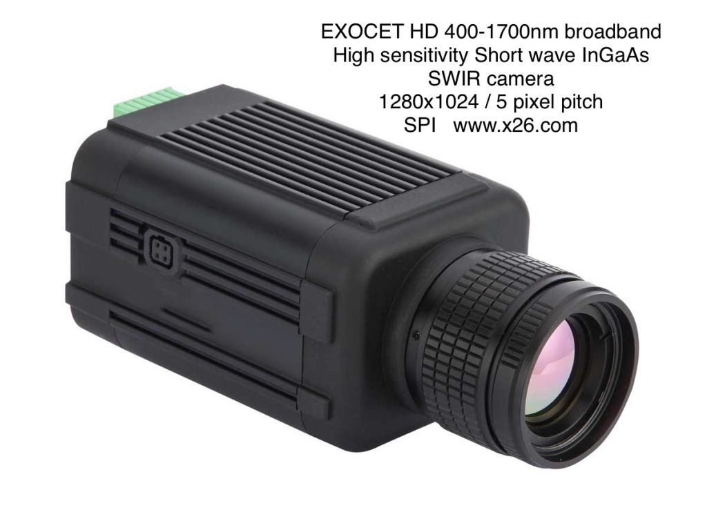 The Exocet SWIR camera is a cost effective High resolution,
ultra sensitive HD SWIR (Short Wave Infrared) camera system used for laser detection, night vision, industrial and commercial inspection applications.
- Seamless image acquisition covering a wide range from visible to HD SWIR
- Broadband VIS-NIR-SWIR 400-1700 nm wavelength high resolution, high sensitivity imaging system
- Advanced InGaAs technology
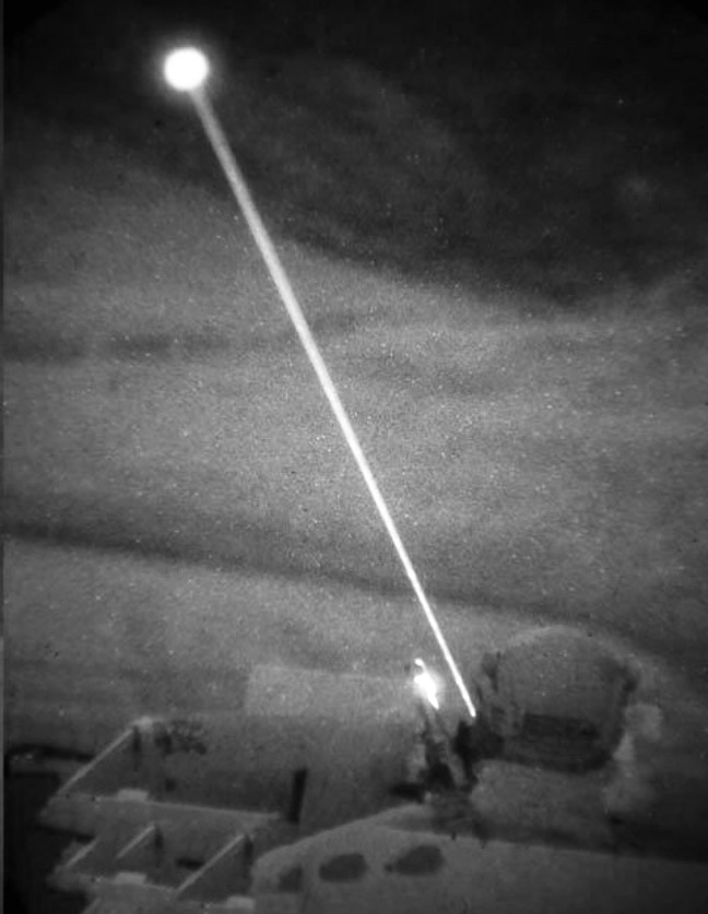
- Remain invisible which painting targets of interest
- Cost effective broadband multi wavelength SWIR camera for sale
- Ultra High sensitivity short wave infrared IR camera used for a wide variety of applications like cutting through atmospheric clutter, military, security, ISR, night vision to specialty inspections
- High-resolution HD 1280 x 1024
- Supports both GigE and CameraLink interfaces.
- Robust digital night vision with sky glow absorption
- Versatile camera for See spot out of band IR JTAC 1064 nanometer IR laser R&D, laser line detection, profiling, analysis, imaging in lab, day, dusk, twilight, sunny bright days, night and total darkness.
10B. Our X27 ultra sensitive HD 400-1200nm broadband extreme low light color night vision NIR camera system has exceptional IR 1064 nm laser Seespot analysis detection and classification capabilities 24/7 in day and night. - Multiple Exotic uses that require specialty broad-band imaging camera systems for ISR related to commercial, industrial, law enforcement, homeland security and military applications.
- Outstanding performance, sensitivity and reliability.
There has been an increasing need for more accurate SWIR cameras in the field of Night vision, surveillance, laser detection, security, semiconductor, agricultural, foods, and medical to name a few. The newly developed advanced Exocet SWIR camera allows for VIS-NIR and SWIR bands to be covered by one robust camera. Short Wave Infrared (SWIR) cameras are ideal for outdoor surveillance applications requiring imaging in low light or for seeing through fog or smoke. SWIR cameras also excel at material inspection and quality assurance tasks such as photovoltaic and semiconductor inspection. Laser Detection & Characterization applications like component alignment and laser beam profiling are also well suited to SWIR cameras.
CLICK HERE FOR THE LASERPRO SWIR
ADVANCED LASER PROFILING
ALL IN ONE MEASUREMENT SUITE
| Model | EXOCET HD SWIR camera |
|---|---|
| SWIR Sensor | Resolution : 1280(H) x 1024(V) Pixel size : 5um x 5um Effective chip size : 6.4mm x 5.12mm |
| Sensor Type | InGaAs Focal Plane Array (FPA) |
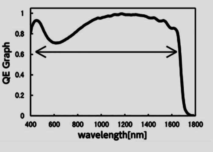
| Spectral range | 400nm ~ 1700nm |
| Interface | Gigabit Ethernet (1000BASE-T) / CameraLink |
| Shutter | Global shutter system |
| Frame rate | CameraLink : Up to 134.7fps (8bit) / 71.5fps (12bit) Gig.E : Up to 61fps (8bit) / 30.5fps (12bit) |
| Main functions | Status LED, internal cooling mechanism, external trigger, ROI, field upgrade function various correction functions (DSNU, PRNU, pixel defect, shading, LUT) |
| Cooling | Single-stage thermoelectric cooling (TEC1) |
| Trigger | Internal/External, LVTTL input 1, Open collector output 4, EIA-422 input 2 (can also be used with LVTTL input2) |
| Gain | 0dB ~ +12dB |
| Input Voltage | DC +12V ~ DC+24V ± 1V |
| Power consumption | TBD |
| Lens mount | C-mount |
| Dimension | 58(W) x 58(H) x 90(D) mm |
Reference SWIR camera data
A benefit of SWIR imaging that is unmatched by other technologies is the ability to image through glass.
- High sensitivity
- High resolution
- Ideal for SWIR laser Profiling and Low light imaging applications (Covert 1550nm illumination)
- Seeing in the light of night glow or night sky radiance
- Day-to-night imaging
- Covert illumination
- Able to see covert lasers and beacons
- No cryogenic cooling required
- Conventional, low-cost visible spectrum lenses
- Small size
- Low power
LONG RANGE InGaAs SWIR camera sensors can be made extremely sensitive, literally counting individual photons. Thus, when built as focal plane arrays with thousands or millions of tiny point sensors, or sensor pixels. Short-wave infrared (SWIR) light is typically defined as light in the 0.9 – 1.7μm wavelength range, but can also be classified from 0.7 – 2.5μm.
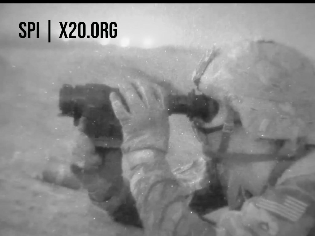
LONG RANGE SWIR Short wave IR can be used for digital night vision applications and to sense IR lasers not seen by night vision goggles, such as 1550 nm and 1064 nm, out of band, see spot and JTAC lasers can be detected in the day and night with the EXOCET HD SWIR camera.
Since silicon sensors have an upper limit of approximately 1.0μm, SWIR imaging requires unique optical and electronic components capable of performing in the specific SWIR range. Indium gallium arsenide (inGaAs) sensors are the primary sensors used in SWIR imaging, covering the typical SWIR range, but can extend as low as 550nm to as high as 2.5μm, a large number of applications that are difficult or impossible to perform using visible light are possible using SWIR. When imaging in SWIR, water vapor, fog, and certain materials such as silicon are transparent. Additionally, colors that appear almost identical in the visible may be easily differentiated using SWIR.
LONG RANGE HD SWIR cameras will work in very dark conditions. Night vision goggles have been around for several decades and operate by sensing and amplifying reflected visible starlight, or other ambient light, in what are called image intensification (I2) tubes. This technology has worked well for direct view night vision goggles. But when an image needs to be sent to a remote location (an intelligence center, for example), there is no practical method which does not introduce reliability and sensitivity limitations (e.g. I2CCD). Using SWIR cameras at night has another major advantage. An atmospheric phenomenon called night sky radiance emits five to seven times more illumination than starlight, nearly all of it in the SWIR wavelengths, with a SWIR camera and this night radiance – often called nightglow, objects can be seen with great clarity on moonless nights and share these images across networks as no other imaging device can do. Short wave infared SWIR InGaAs cameras can be small and use very little power, but give big results. InGaAs Cameras found early applications in the telecom industry because it is sensitive to the light used in long distance fiber optics communications, usually around 1550 nm. By using SWIR illumination like 1.55 micron lasers or LEDs, it is possible to covertly illuminate a scene that can be viewed only with SWIR cameras. SWIR InGaAs cameras are of great value in such applications. SWIR imaging is used in a variety of applications including electronic board inspection, solar cell inspection, produce inspection, identifying and sorting, surveillance, anti-counterfeiting, process quality control, and much more.
LONG RANGE HD SWIR light interacts with objects similarly to visible light as it is reflective, consequently it exhibits shadows and contrasts in its imagery. Images from a SWIR camera are comparable to visible images in terms of resolution and detail.
Objects that are almost the same color while imaging in visible region can be easily differentiated using SWIR light, making objects easily recognizable. This is one tactical advantage of imaging in SWIR compared to visible region. Some of the natural emitters of SWIR are ambient star light and background radiance, therefore SWIR is an excellent application for outdoor imaging. Conventional quartz/halogen bulbs also act as a SWIR light source. Depending on the application, some sensors in SWIR cameras can be adjusted to have linear or logarithmic response to avoid saturation.
There are many advantages of using HD LONG RANGE SWIR over a conventional visible sensor. Some applications that are not possible to image in visible range can be imaged using SWIR range. One example, is silicon wafer inspection, which is only possible due to silicon being transparent in the SWIR range. Other examples of materials that are transparent in SWIR region are; Sodium Chloride (NaCl) and Quartz (SiO2). Water vapor is also transparent in SWIR, making SWIR cameras more desirable when imaging through haze or fog. SWIR is the acronym for shortwave infrared and refers to non-visible light falling roughly between 1400 and 3000 nanometers (nm) in wavelength. The visible spectrum ranges from 400nm to 700nm, therefore SWIR light is invisible to the human eye. In order to detect SWIR wavelengths, we need dedicated sensors made of In GaAs (Indium Gallium Arsenide) or MCT (mercury cadmium Telluride) as silicon detectors are no longer sensitive to wavelengths larger than 1100 nm. In GaAs sensors are the primary sensors used in typical SWIR range. MCT is also an option and can extend the SWIR range, but these sensors are usually more costly and application dependent. SWIR typically defines wavelengths between 900 and 1700 nm. Extended SWIR or eSWIR defines wavelengths that go beyond the standard 1.75µm of InGaAs sensors. eSWIR can go up to 2.2 or 2.5 µm. Visible SWIR or vSWIR defines the part of the spectrum including both visible and swir wavelengths. vSWIR typically covers 400 to 1700 nm. InGaAs cameras bridge the gap between NIR wavelengths in the 950-1700 nm range, where silicon detectors are no longer sensitive. There is a still a gap however in the resolution of InGaAs sensors compared to that of silicon detectors, which can nowadays reach tens of megapixels and sometimes over 100 megapixels.
There are 3 resolutions for SWIR InGaAs sensors on the market, with price increasing as the resolution goes up. Sensor pixel pitch is often related to the resolution with higher resolution sensors tending to have smaller pixels.
QVGA sensors offer a resolution of 320 (H) by 256 (V) pixels with a pixel pitch typically ranging from 20µm to 30µm.
VGA sensors are today the most standard resolution for InGaAs sensors with a resolution of 640(H) by 512 (V) pixels and a typical pixel pitch of 15µm. SWIR cameras are used for a variety of applications in different aspects of the industry and research, ranging from inspection, quality control, identification, detection, surveillance, and more. Here we summarize some applications where SWIR range is commonly used. More applications are being discovered all the time.
New HD SWIR is coming out with a pixel pitch of 5µm, making them the smallest pixel pitch on the market for InGaAs-based sensors. High resolution imaging is now possible with 1280 (H) x 1024 (V) or 640 (H) x 512 (V) resolution sensors with 5µm pixel pitch.
Measurement and analysis of laser-beam characteristics is essential for today’s laser-based applications. In general, beam characterization involves measurement of the beam spatial-energy density distribution, commonly known as the beam profile. Beam-profile analysis provides an understanding of the beam spatial characteristics such as size, shape, position, propagation, and mode structure properties. These measurements enable the required process-specific beam parameters, such as alignment, focus spot size, or beam uniformity (to name a few), to be achieved and maintained for optimum laser system performance.
For lasers with beams that are nearly collimated (paraxial), measurement of the beam-profile characteristics involves sampling the spatial distribution of the beam energy (or power) density in a plane (x and y-axis) perpendicular to the beam propagation path.
The advent of two-dimensional long range hd Ptz InGaAs detector arrays offers a viable approach for measurement of short-term beam-profile variations as opposed to scanning slit based systems. The individual sensors (pixels) in the detector arrays provide measurement of the energy density at discrete locations across the entire beam measurement plane while the entire array samples the beam simultaneously, thus providing a virtually instantaneous two-dimensional beam-profile data set (or beam image).
FSO can be used for ground to ground communication: outdoor wireless 2G/3G and 4G networks, to cover the edge of physical networks (“the last mile access”), CCTV surveillance networks, etc. More importantly, it can be used for ground to space (satellite) communications. FSO enables simultaneously establishing a large number of independent links with high throughput; two major advantages compared to the radio bandwidth which is limited by its low directionality and radio frequency throughput (< 40 GHz). For example, Earth-observation satellites only overpass ground stations for a couple of minutes per day, it is critical that the large amount of data they collected can be transmitted in a short amount of time. Even more so for military satellites which very often may only communicate with ground stations within a limited geographical zone. Finally, FSO is the best option for extra-terrestrial communication which may come in use in the next decades… In short, FSO is a fast-growing segment for telecommunications, both in civil and military fields.
FSO communications are limited by a series of factors. Fortunately, some can be overcome by using Short Wave InfraRed (SWIR) (900 – 1700 nm) rather than visible (400 – 700 nm) or Near InfraRed (700 – 900 nm) wavelengths. Optimized transmission Disturbances inherent to air/free space may influence the optical transmission:
- weather conditions such as fog, rain, snow…
- various other effects like water/dust absorption, scintillation, scattering
- physical obstruction: trees, birds or buildings.
These factors attenuate the transmitted signal, leading to a higher number of errors when detecting the signal. Laser power increase is not the solution as the laser power density is limited to class 1M in order to keep an eye-safe environment.
The use of SWIR band lasers is extremely pertinent because of their ability to go through obstacles such as fog or some types of plastics. The recent rise of eye-safe lasers in the SWIR band has allowed a major improvement. A camera based on an InGaAs detector array must be used at the receiver end, as visible cameras are not sensitive to SWIR wavelengths.
An FSO system in its simplest form is illustrated below. The data to be transmitted is converted to a binary format (1 and 0), then into light pulses (ON/OFF). A transmitter (laser source and focusing lens) sends the light pulses, aiming the direction of a receiver. The receiver collects the light pulses, which are then processed and converted. Note that the system can be used in the reverse direction. The system is interfaced at both ends with a physical network (cable, fiber). In more complex implementations, the laser beam can be modulated.
This approach can therefore capture the beam characteristics of a single laser pulse. When coupled to a computer, the detector-array data can be digitized and graphically displayed for qualitative visual inspection of the beam mode profile structure using a variety of beam profile plots. Numerical analysis of the profile data provides information;
- Position: peak position, centroid position;
- Relative total energy or power;
- Mode structure analysis: Gaussian fits, top-hat fits, uniformity, satellite or stray beams and more.
- Peak power or energy density;
- Width and diameter: knife-edge, slit, D86, second moment (D4σ), cross-section widths, fitted widths and more;
- Circularity/ellipticity, aspect ratio, beam orientation;
- Divergence (requires far-field optical set-up or a focusing lens)
- Propagation M2, beam parameter product (requires multiple profile measurements through beam waist).Small animal imaging is one of the main research areas for preclinical studies, including but not limited to; drug discovery, drug effectiveness, and early detection of cancer. Over time, imaging in the SWIR range became more profitable for scientists studying small animals. The short wave infrared (SWIR) range has several advantages compared to visible and infrared wavelengths in the domain of in vivo imaging. SWIR light provides higher depth of penetration while maintaining high resolution, low light absorption and reduced scattering within the tissue which makes it desirable to study living organisms. One of the biggest advantages of the SWIR range is that the auto fluorescence is negligible. This low level auto fluorescence increases the contrast and sensitivity compared to conventional imaging in NIR and visible ranges. Some of NIR fluorescence imaging contrast agents such as; ICG (indocyanine green), IRDye800CW and IR-12N3, has a non-negligible long tails passing 1500 nm region (NIR-II/SWIR), InGaAs (indium gallium arsenide) based SWIR cameras fill the gap for imaging in NIR-II/SWIR wavelength range (900-1700nm) where silicon detectors are no longer sensitive.
SWIR cameras can be used for detection of single-walled carbon nanotubes requiring fast frame rates. Single-walled carbon nanotubes (SWCNT) have been established as remarkable fluorophores for probing the nanoscale organization of biological tissues [1,2]. They are stiff, quasi-one-dimensional nano structures, with a small diameter (~1nm) which enables excellent penetration into complex environments, and a large length (100nm to 1µm) which slows down their diffusion and thus allows the tracking of single fluorescent particles. Finally, their bright and stable near-infrared (NIR) fluorescence allows long-term tracking deep in biological tissues without suffering from biological autofluorescence. For example, single-walled carbon nanotubes could be detected in distant regions of the brain extracellular space (ECS) following their injection into the lateral ventricles of young rat brains, and the tracking of their diffusion. This yields novel and quantitative insights about the local morphology and viscosity variations within the brain ECS[1,2]. Such studies require a camera capable of tracking single-walled carbon nanotubes at high speed, making SWIR cameras desirable. One limiting factor for the spatial resolution of such diffusion analyses is the ability to observe displacements of SWCNTs over short time lags.SWIR cameras can be used for thermal imaging of hot objects between 250°C and 800°C. The metal and glass industry integrates SWIR cameras into process and quality control systems.In contrast to CCD and CMOS cameras, the spectral range of a typical InGaAs camera of 900 nm to 1,700 nm enables the inspection of emission differences between hot metal and slag. The information is used to detect differences in the slag within the manufacturing process. This ensures a maximized yield without any contaminated material. Glass bottle monitoring and inspection During the manufacturing process of bottles, InGaAs cameras enable an inside and outside inspection of the glass bottles. Because of their ability to perform thermal imaging of hot objects between 250°C and 800°C, SWIR cameras can monitor the temperature uniformity and the cooling rate of the glass. Thus, manufacturers can continuously observe the production to maximize the yield and the quality.
The semiconductor industry has become one of the largest industries in the world and continues to expand. Manufacturing integrated circuits (ICs or chips) on thin silicon discs (wafers) is at the heart of this industry. Cameras with InGaAs sensors typically operate in the hd SWIR spectral range between 900 nm and 1,700 nm and can image through semiconductor materials such as silicon (Si) at wavelengths around 1,150 nm. Thus, they are an essential part of the inspection process. The ability to image through Si provides a non-destructive inspection method with great benefits for the production process. Today, the semi conductor industry integrates InGaAs cameras into testing, inspection, and quality control systems. Silicon crystal and ingot brick inspection Inspecting silicon crystals and ingots (also called bricks) is one of the classic applications for InGaAs cameras in the semiconductor industry. The ability to see through silicon at a wavelength range above 1,150 nm makes InGaAs cameras a well-suited solution for detecting inclusions such as impurities within a crystal or ingot, which can accumulate during the production process. The impurities are critical when sawing the ingots into thin wafers with a special diamond chain. If the chain strikes an inclusion such as a small piece of metal, the extremely expensive chain can break. Not only does replacing a chain carry a cost, but also leads to a lower productivity and a reduced profit. A SWIR camera can prevent this situation and thus ensure a smooth production process.
Metal & Glass Industry
SWIR cameras can be used for thermal imaging of hot objects between 250°C and 800°C. The metal and glass industry integrates SWIR cameras into process and quality control systems.
Molten metal process monitoring and inspection
In contrast to CCD and CMOS cameras, the spectral range of a typical InGaAs camera of 900 nm to 1,700 nm enables the inspection of emission differences between hot metal and slag. The information is used to detect differences in the slag within the manufacturing process. This ensures a maximized yield without any contaminated material.
Glass bottle monitoring and inspection
During the manufacturing process of bottles, InGaAs cameras enable an inside and outside inspection of the glass bottles. Because of their ability to perform thermal imaging of hot objects between 250°C and 800°C, SWIR cameras can monitor the temperature uniformity and the cooling rate of the glass. Thus, manufacturers can continuously observe the production to maximize the yield and the quality.
Wafer inspection or packaging
Another important application for SWIR cameras is the wafer inspection. During the manufacturing process of wafers, particles may occur on the top, at the bottom, and even inside or between the wafers. Whereas CCD or CMOS cameras detect particles on the top and at the bottom, InGaAs cameras see through the silicon and therefore detect particles between two bonded wafers. InGaAs cameras are also used for wafer packaging, where the alignment of the backside pattern to the front side of the wafer is conducted. The SWIR technology helps align layers of wafers as well as aligning other sub products such as ICs, memory cells, or transistors along the entire supply chain.
We are here to help assist you in selecting the absolute highest quality, cost effective
day/night video security/surveillance system for your needs.
Additional Long range thermal cameras
are available at this LINK
Click here for the history and terminology related to thermal
infrared flir imaging and night vision equipment.
Long range thermal imaging flir PTZ camera resources
CALL (702) 499-9551 OR EMAIL US FOR
ADDITIONAL INFO AND DISCOUNTED PRICING